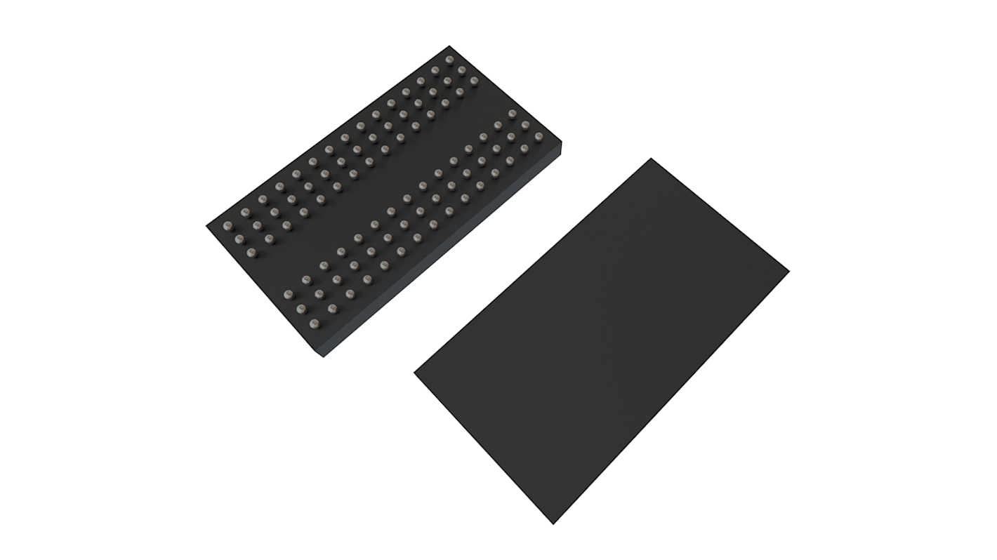
SDRAM Winbond 128Mbit DDR2

- RS品番:
- 188-2730
- メーカー型番:
- W9712G6KB25I
- メーカー/ブランド名:
- Winbond
一時的な在庫切れ - 2024/11/29に入荷し、その後4営業日でお届け予定
追加されました
単価: 購入単位は5個
¥390.60
(税抜)
¥429.66
(税込)
| 個 | 単価 | 購入単位毎合計* |
| 5 - 5 | ¥390.60 | ¥1,953.00 |
| 10 - 95 | ¥379.20 | ¥1,896.00 |
| 100 - 125 | ¥365.20 | ¥1,826.00 |
| 130 - 170 | ¥314.80 | ¥1,574.00 |
| 175 + | ¥304.20 | ¥1,521.00 |
| * 購入単位ごとの価格 | ||
- RS品番:
- 188-2730
- メーカー型番:
- W9712G6KB25I
- メーカー/ブランド名:
- Winbond
データシート
その他
詳細情報
The W9712G6KB is a 128M bits DDR2 SDRAM and speed involving -25, 25I and -3.
Double Data Rate architecture: two data transfers per clock cycle
CAS Latency: 3, 4, 5 and 6
Burst Length: 4 and 8
Bi-directional, differential data strobes (DQS and /DQS ) are transmitted / received with data
Edge-aligned with Read data and center-aligned with Write data
DLL aligns DQ and DQS transitions with clock
Differential clock inputs (CLK and /CLK)
Data masks (DM) for write data
Commands entered on each positive CLK edge, data and data mask are referenced to both edges of /DQS
Posted /CAS programmable additive latency supported to make command and data bus efficiency
Read Latency = Additive Latency plus CAS Latency (RL = AL + CL)
Off-Chip-Driver impedance adjustment (OCD) and On-Die-Termination (ODT) for better signal quality
Auto-precharge operation for read and write bursts
Auto Refresh and Self Refresh modes
Precharged Power Down and Active Power Down
Write Data Mask
Write Latency = Read Latency - 1 (WL = RL - 1)
Interface: SSTL_18
受注確定後にお客様専用製品として商品化されるため、発注後のキャンセル・返品はお受けできません。
仕様
特性 | |
|---|---|
| メモリサイズ | 128Mbit |
| SDRAMクラス | DDR2 |
| 構成 | 16M x 8 bit |
| データレート | 200MHz |
| データバス幅 | 16bit |
| アドレスバス幅 | 15bit |
| 1ワード当たりのビット数 | 8bit |
| 最大ランダムアクセス時間 | 0.4ns |
| ワード数 | 16M |
| 実装タイプ | 表面実装 |
| パッケージタイプ | TFBGA |
| ピン数 | 84 |
| 寸法 | 12.6 x 8.1 x 0.8mm |
| 高さ | 0.8mm |
| 長さ | 12.6mm |
| 動作温度 Min | -40 °C |
| 動作供給電圧 Min | 1.7 V |
| 動作温度 Max | +95 °C |
| 幅 | 8.1mm |
| 動作供給電圧 Max | 1.9 V |