onsemi MOSFET, Nチャンネル, 17 A, 表面実装, 4 ピン, FCMT180N65S3
- RS品番:
- 178-4240
- メーカー型番:
- FCMT180N65S3
- メーカー/ブランド名:
- onsemi

在庫が表示されていない場合があります。ページの再読み込みをお試しください。
- RS品番:
- 178-4240
- メーカー型番:
- FCMT180N65S3
- メーカー/ブランド名:
- onsemi
仕様
データシート
その他
詳細情報
製品情報(複数選択可)を選択して、類似製品を検索します。
すべて選択 | 製品情報 | 内容 |
|---|---|---|
| ブランド | onsemi | |
| チャンネルタイプ | N | |
| 最大連続ドレイン電流 | 17 A | |
| 最大ドレイン-ソース間電圧 | 650 V | |
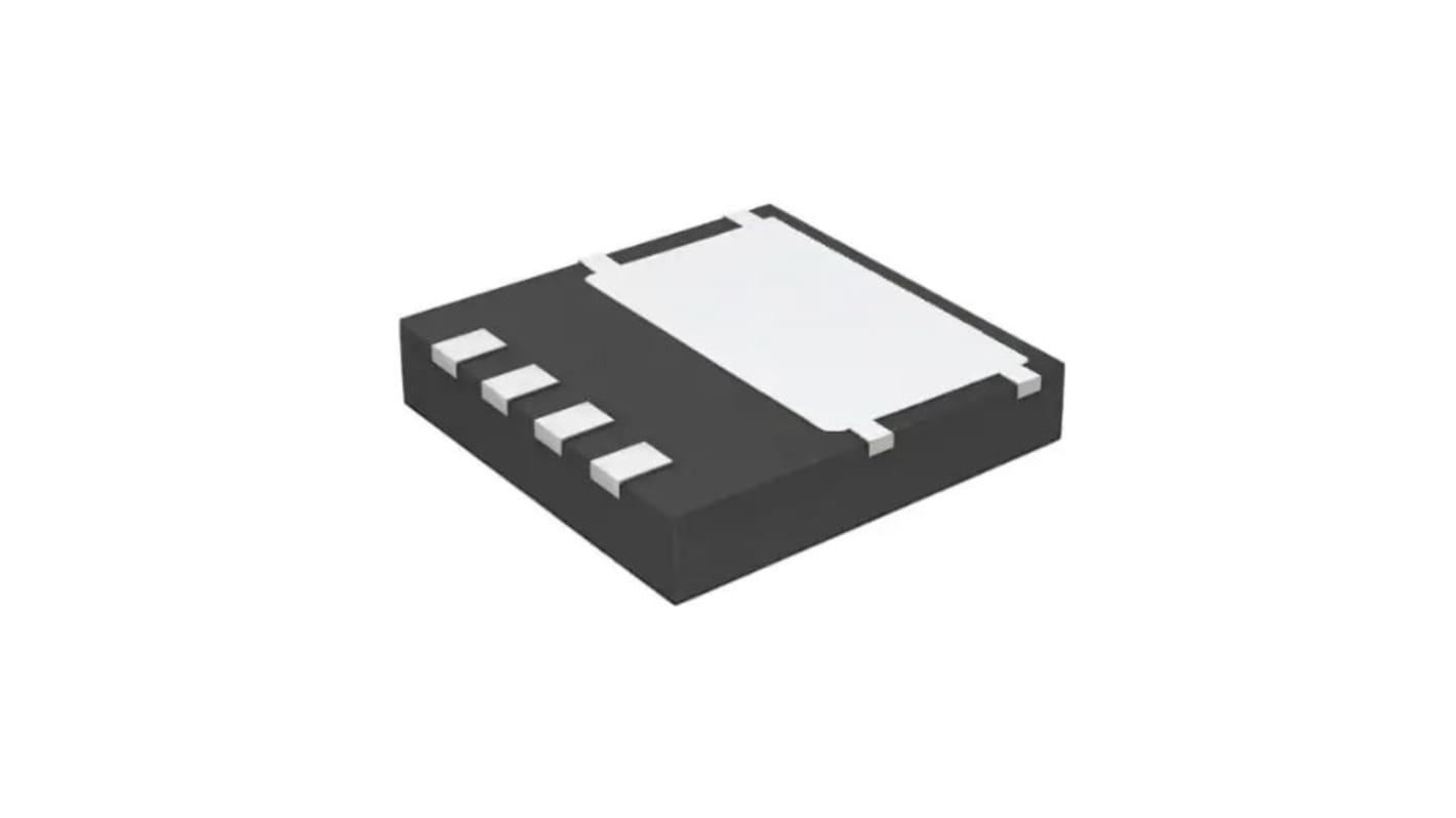
| パッケージタイプ | Power88 | |
| 実装タイプ | 表面実装 | |
| ピン数 | 4 | |
| 最大ドレイン-ソース間抵抗 | 180 mΩ | |
| チャンネルモード | エンハンスメント型 | |
| 最大ゲートしきい値電圧 | 4.5V | |
| 最低ゲートしきい値電圧 | 2.5V | |
| 最大パワー消費 | 139 W | |
| トランジスタ構成 | シングル | |
| 最大ゲート-ソース間電圧 | ±30 V | |
| 幅 | 8mm | |
| 標準ゲートチャージ @ Vgs | 33 nC @ 10 V | |
| 長さ | 8mm | |
| 動作温度 Max | +150 °C | |
| 1チップ当たりのエレメント数 | 1 | |
| 動作温度 Min | -55 °C | |
| 順方向ダイオード電圧 | 1.2V | |
| 高さ | 1.05mm | |
| すべて選択 | ||
|---|---|---|
ブランド onsemi | ||
チャンネルタイプ N | ||
最大連続ドレイン電流 17 A | ||
最大ドレイン-ソース間電圧 650 V | ||
パッケージタイプ Power88 | ||
実装タイプ 表面実装 | ||
ピン数 4 | ||
最大ドレイン-ソース間抵抗 180 mΩ | ||
チャンネルモード エンハンスメント型 | ||
最大ゲートしきい値電圧 4.5V | ||
最低ゲートしきい値電圧 2.5V | ||
最大パワー消費 139 W | ||
トランジスタ構成 シングル | ||
最大ゲート-ソース間電圧 ±30 V | ||
幅 8mm | ||
標準ゲートチャージ @ Vgs 33 nC @ 10 V | ||
長さ 8mm | ||
動作温度 Max +150 °C | ||
1チップ当たりのエレメント数 1 | ||
動作温度 Min -55 °C | ||
順方向ダイオード電圧 1.2V | ||
高さ 1.05mm | ||
- COO(原産国):
- PH
SUPERFET III MOSFET is ON Semiconductor’s brand−new high voltage super−junction (SJ) MOSFET family that is utilizing charge balance technology for outstanding low on−resistance and lower gate charge performance. This advanced technology is tailored to minimize conduction loss, provide superior switching performance, and withstand extreme dv/dt rate.
700 V @ TJ = 150 oC
Leadless Ultra-thin SMD package
Kelvin contact
Ultra Low Gate Charge (Typ. Qg = 33 nC)
Low Effective Output Capacitance (Typ. Coss(eff.) = 305 pF)
Optimized Capacitance
Typ. RDS(on) = 152 mΩ
Moisture Sensitivity Level 1 guarantee
Internal Gate Resistance: 0.5 Ω
Benefits:
Higher system reliability at low temperature operation
High power density
Low gate noise and switching loss
Low switching loss
Low switching loss
Lower peak Vds and lower Vgs oscillation
Applications:
Computing
Telecommunication
Industrial
End Products:
Telecom / Server
Adapter
LED Lighting
受注確定後にお客様専用製品として商品化されるため、発注後のキャンセル・返品はお受けできません。
関連ページ
- onsemi MOSFET 24 A エンハンスメント型 4-Pin パッケージPQFN, FCMT125N65S3
- onsemi MOSFET 10 A エンハンスメント型 4-Pin パッケージPQFN, FCMT360N65S3
- onsemi MOSFET 12 A エンハンスメント型 4-Pin パッケージPower88, FCMT250N65S3
- onsemi MOSFET 24 A エンハンスメント型 4-Pin パッケージPQFN
- onsemi MOSFET 10 A エンハンスメント型 4-Pin パッケージPQFN
- onsemi MOSFET 12 A エンハンスメント型 4-Pin パッケージPower88
- onsemi MOSFET 16 A 3 ピン, FQP17N40
- onsemi MOSFET 17 A エンハンスメント型 3-Pin パッケージTO-220, FCP190N65S3