Winbond SDRAM, 512Mbit, LPDDR, 200MHz, W949D2DBJX5I
- RS品番:
- 188-2651P
- メーカー型番:
- W949D2DBJX5I
- メーカー/ブランド名:
- Winbond

取扱終了
在庫限りでお取扱いは終了致します。
- RS品番:
- 188-2651P
- メーカー型番:
- W949D2DBJX5I
- メーカー/ブランド名:
- Winbond
仕様
データシート
その他
詳細情報
製品情報(複数選択可)を選択して、類似製品を検索します。
すべて選択 | 製品情報 | 内容 |
|---|---|---|
| ブランド | Winbond | |
| メモリサイズ | 512Mbit | |
| 構成 | 64 M x 8 ビット | |
| SDRAMクラス | LPDDR | |
| データレート | 200MHz | |
| データバス幅 | 32bit | |
| アドレスバス幅 | 15bit | |
| 1ワード当たりのビット数 | 8bit | |
| 最大ランダムアクセス時間 | 5ns | |
| ワード数 | 64M | |
| 実装タイプ | 表面実装 | |
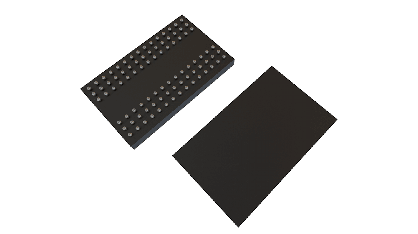
| パッケージタイプ | VFBGA | |
| ピン数 | 90 | |
| 寸法 | 13.1 x 8.1 x 0.65mm | |
| 高さ | 0.65mm | |
| 長さ | 13.1mm | |
| 動作温度 Min | -40°C | |
| 動作温度 Max | +85 ℃ | |
| 幅 | 8.1mm | |
| 動作供給電圧 Max | 1.95 V | |
| 動作供給電圧 Min | 1.7 V | |
| すべて選択 | ||
|---|---|---|
ブランド Winbond | ||
メモリサイズ 512Mbit | ||
構成 64 M x 8 ビット | ||
SDRAMクラス LPDDR | ||
データレート 200MHz | ||
データバス幅 32bit | ||
アドレスバス幅 15bit | ||
1ワード当たりのビット数 8bit | ||
最大ランダムアクセス時間 5ns | ||
ワード数 64M | ||
実装タイプ 表面実装 | ||
パッケージタイプ VFBGA | ||
ピン数 90 | ||
寸法 13.1 x 8.1 x 0.65mm | ||
高さ 0.65mm | ||
長さ 13.1mm | ||
動作温度 Min -40°C | ||
動作温度 Max +85 ℃ | ||
幅 8.1mm | ||
動作供給電圧 Max 1.95 V | ||
動作供給電圧 Min 1.7 V | ||
- COO(原産国):
- TW
VDD = 1.7∼1.95V
VDDQ = 1.7∼1.95V
データ幅:x16 / x32
クロックレート:200MHz(-5)、166MHz(-6)
標準セルフ・リフレッシュ・モード
パーシャルアレイセルフリフレッシュ(PASR)
自動温度補償セルフリフレッシュ(ATCSR)
パワーダウンモード
ディープ・パワーダウン・モード(DPDモード)
プログラマブル出力バッファ・ドライバ強度
同時動作のための4つの内部バンク
書き込みデータ用データマスク(DM)
アイドル時のクロック停止機能
各バースト・アクセスの自動プリチャージ・オプション
データ出力は2倍のデータレート
差動クロック入力(CKおよびCK)
双方向、データストローブ(DQS)
CASレイテンシー:2および3
バースト長:2、4、8、16
バーストタイプ:シーケンシャルまたはインターリーブ
8Kリフレッシュ・サイクル/64mS
インターフェースLVCMOS互換
サポートパッケージ:
60ボールVFBGA(x16)
90ボールVFBGA(x32)
動作温度範囲
拡張: -25°C ≤ TCASE ≤ 85°C
産業用: -40°C ≤ TCASE ≤ 85°C
これは512Mbの低消費電力DDR SDRAMで、2Mワードx4バンクx32ビットで構成されている。
バーストタイプ:シーケンシャルまたはインターリーブ
標準セルフ・リフレッシュ・モード
PASR、ATCSR、パワーダウンモード、DPD
プログラマブル出力バッファ・ドライバ強度
同時動作のための4つの内部バンク
双方向、データ・ストローブ(DQS)はデータと共に送受信され、レシーバーでデータを取り込む際に使用される。
標準セルフ・リフレッシュ・モード
PASR、ATCSR、パワーダウンモード、DPD
プログラマブル出力バッファ・ドライバ強度
同時動作のための4つの内部バンク
双方向、データ・ストローブ(DQS)はデータと共に送受信され、レシーバーでデータを取り込む際に使用される。
受注確定後にお客様専用製品として商品化されるため、発注後のキャンセル・返品はお受けできません。