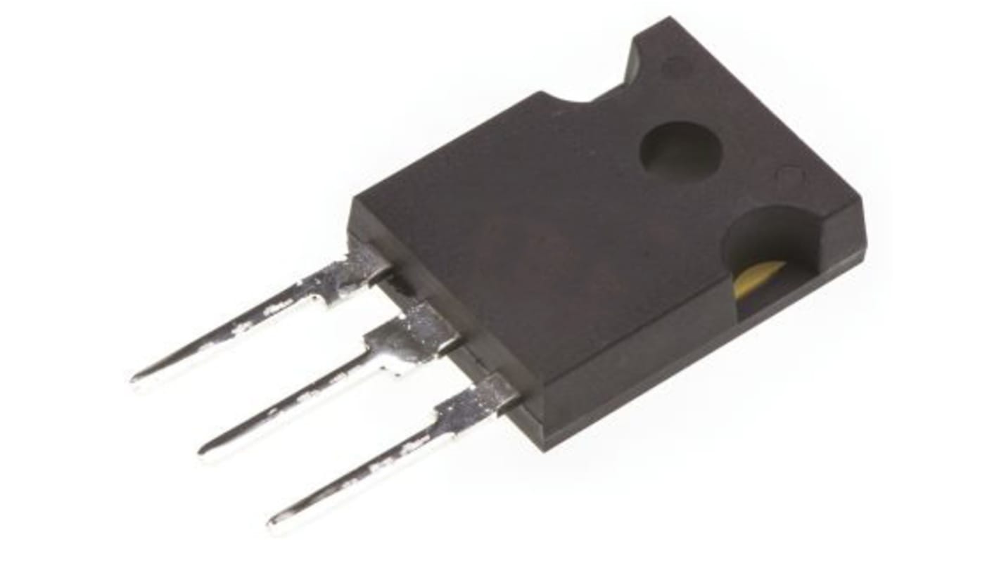
onsemi MOSFET, タイプNチャンネル 650 V, 30 A エンハンスメント型, スルーホール, 3-Pin パッケージTO-247, NTHL110N65S3F
- RS品番:
- 178-4486
- メーカー型番:
- NTHL110N65S3F
- メーカー/ブランド名:
- onsemi

ボリュームディスカウント対象商品
一括購入価格オプションを表示1 袋(1袋2個入り) 小計:*
¥2,517.00
(税抜)
¥2,768.70
(税込)
3,000円を超える注文については、送料無料
在庫あり
- 408 は海外在庫あり
「配達日を確認」をクリックすると、在庫と配送の詳細が表示されます。
個 | 単価 | 購入単位毎合計* |
|---|---|---|
| 2 - 6 | ¥1,258.50 | ¥2,517 |
| 8 - 14 | ¥1,219.50 | ¥2,439 |
| 16 - 18 | ¥1,182.50 | ¥2,365 |
| 20 - 22 | ¥1,144.00 | ¥2,288 |
| 24 + | ¥1,105.00 | ¥2,210 |
* 表示は参考価格です。ご購入数量によって価格は変動します。なお、上記数量を大きく超える大量ご購入の際は右下チャットからお問合せください。
- RS品番:
- 178-4486
- メーカー型番:
- NTHL110N65S3F
- メーカー/ブランド名:
- onsemi
仕様
データシート
その他
詳細情報
製品情報(複数選択可)を選択して、類似製品を検索します。
すべて選択 | 製品情報 | 内容 |
|---|---|---|
| ブランド | onsemi | |
| チャンネルタイプ | タイプN | |
| プロダクトタイプ | MOSFET | |
| 最大連続ドレイン電流Id | 30A | |
| 最大ドレイン-ソース間電圧Vds | 650V | |
| シリーズ | NTHL | |
| パッケージ型式 | TO-247 | |
| 取付タイプ | スルーホール | |
| ピン数 | 3 | |
| 最大ドレイン-ソース間抵抗Rds | 110mΩ | |
| チャンネルモード | エンハンスメント型 | |
| 標準ゲートチャージ Qg @ Vgs | 58nC | |
| 順方向電圧 Vf | 1.3V | |
| 動作温度 Min | -55°C | |
| 最大許容損失Pd | 240W | |
| 動作温度 Max | 150°C | |
| 規格 / 承認 | No | |
| 長さ | 15.87mm | |
| 高さ | 20.82mm | |
| 自動車規格 | なし | |
| すべて選択 | ||
|---|---|---|
ブランド onsemi | ||
チャンネルタイプ タイプN | ||
プロダクトタイプ MOSFET | ||
最大連続ドレイン電流Id 30A | ||
最大ドレイン-ソース間電圧Vds 650V | ||
シリーズ NTHL | ||
パッケージ型式 TO-247 | ||
取付タイプ スルーホール | ||
ピン数 3 | ||
最大ドレイン-ソース間抵抗Rds 110mΩ | ||
チャンネルモード エンハンスメント型 | ||
標準ゲートチャージ Qg @ Vgs 58nC | ||
順方向電圧 Vf 1.3V | ||
動作温度 Min -55°C | ||
最大許容損失Pd 240W | ||
動作温度 Max 150°C | ||
規格 / 承認 No | ||
長さ 15.87mm | ||
高さ 20.82mm | ||
自動車規格 なし | ||
- COO(原産国):
- CN
SUPERFET III MOSFET is ON Semiconductor’s brand−new high voltage super−junction (SJ) MOSFET family that is utilizing charge balance technology for outstanding low on−resistance and lower gate charge performance. This advanced technology is tailored to minimize conduction loss, provide superior switching performance, and withstand extreme dv/dt rate.
Features:
700 V @ TJ = 150 °C
Ultra Low Gate Charge (Typ. Qg = 58 nC)
Low Effective Output Capacitance (Typ. Coss(eff.) = 553 pF)
Excellent body diode performance (low Qrr, robust body diode)
Optimized Capacitance
Typ. RDS(on) = 98 mΩ
Benefits:
Higher system reliability at low temperature operation
Lower switching loss
Lower switching loss
Higher system reliability in LLC and Phase shift full bridge circuit
Lower peak Vds and lower Vgs oscillation
Applications:
Telecommunication
Cloud system
Industrial
End Products:
Telecom power
Server power
EV charger
Solar / UPS
関連ページ
- onsemi MOSFET 30 A エンハンスメント型 3-Pin パッケージTO-247
- onsemi MOSFET 75 A エンハンスメント型 3-Pin パッケージTO-247, NTHL027N65S3HF
- onsemi MOSFET 24 A エンハンスメント型 3-Pin パッケージTO-247, NTHL125N65S3H
- onsemi MOSFET 30 A エンハンスメント型 3-Pin パッケージTO-247, NTHL095N65S3H
- onsemi MOSFET 40 A エンハンスメント型 3-Pin パッケージTO-247, NTHL067N65S3H
- onsemi MOSFET 46 A エンハンスメント型 3-Pin パッケージTO-247, NTHL065N65S3F
- onsemi MOSFET 20 A エンハンスメント型 3-Pin パッケージTO-247, NTHL190N65S3HF
- onsemi MOSFET 65 A エンハンスメント型 3-Pin パッケージTO-247, NTHL040N65S3F